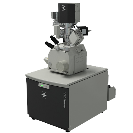
Vion Plasma Focused Ion Beam
The FEI Vion™ Plasma Focused Ion Beam System (PFIB) adds significantly more capacity to your lab, with best-in-class milling and imaging performance in a single, easy-to-use instrument. By incorporating plasma ion source technology, the Vion PFIB delivers increased throughput over conventional gallium FIB instruments-with speeds more than 20x faster for site-specific cross-sectioning and large area milling, as well as sample preparation. With both excellent milling precision and high-resolution imaging at low beam currents, the Vion PFIB delivers the speed, accuracy and high contrast images essential for a wide range of process control, failure analysis or materials research applications.
.png)
Vion PFIB for Materials Science
Especially well-suited for metals, composites and coatings, the Vion PFIB supports a range of materials characterization, failure analysis and sample preparation applications.
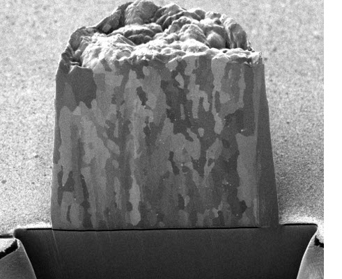
- Create site-specific cross sections quickly while directly imaging samples for real-time monitoring
- Achieve greater milling speed without sacrificing quality for large area and repetitive milling projects, as well as for low sputter rate materials like steel
- Perform fast, site-specific micromachining of structures and surfaces for dynamic compression or tensile testing.
- Prepare high quality, site-specific surfaces for Electron Back Scattered Diffraction analysis Prepare specimens for other imaging and characterization techniques like SEM and TEM
- Gain sub-30 nm image resolution for quick identification and metrology of thin layers and structures.
Product Models
Vion PFIB for Electronics
High Throughput 3D Packaging Analysis
The Vion plasma FIB is an instrument capable of highly precise high-speed cutting and milling. It has the ability to selectively mill areas of interest. In addition, the PFIB can selectively deposit patterned conductors and insulators.
By combining high-speed milling with precise control, the system can be used in several ways for manufacturing of IC's, such as:
- * Failure analysis of bumps, wire bonds, TSVs, and stacked die
- * Surgically remove package and material to enable failure analysis and fault isolate on buried die
- * For process monitoring and development at package level
- * Defect analysis of packaged parts and MEMS devices